Top 5 Challenges In HDI PCB Design
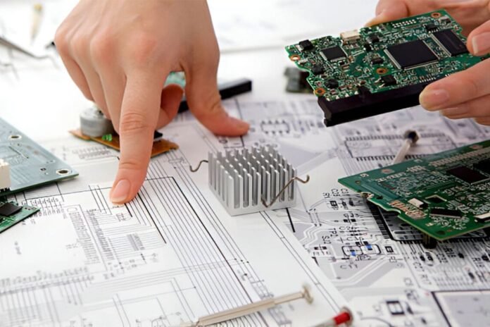
The global demand for faster, smaller and lighter devices has boosted the growth of Printed Circuit Board (PCB) technology. Electronic devices are advancing with the passage of time with the adoption of 5G, Artificial Intelligence (AI) and automation. PCBs can come in various forms, from simple, one-layer electronic boards to more complex designs such as multi-layered boards.
As complexity has inevitably increased, another type of PCB known as HDI PCB, has been developed. This PCB type is able to support more efficient and miniaturized technologies in the area of electronics. The HDI market is projected to grow with the increasing need for electronic devices in consumer, industrial, automotive, medical and many more. In this article, we will have more insights about HDI circuit boards, and the top challenges usually encountered in this type of printed circuit board.
What Is HDI PCB?
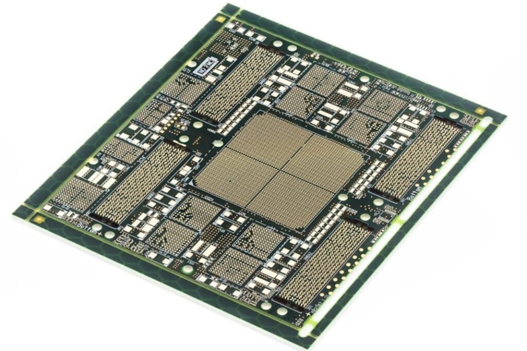
An HDI PCB is short for High Density Interconnect Printed Circuit Board, which is a type of PCB with heavily populated components, complex circuitry and dense electronics. Some of its features include laser-drilled micro-vias, fine conductive tracks and a series of lamination structures.
The complexity of HDI PCB design circuit boards is a result of the necessity for higher pin counts, better routing and signal integrity, and high-speed technologies. Imaging and etching processes are enhanced for better registration with tighter tolerances and better resolution.
What Are The Top 5 Challenges In HDI PCB Design?
Here are the top 5 challenges that one must look out for when designing HDI PCBs.
1. Setting Up Signal Routings
Signal integrity can be an issue if the distances and positions of signal routings are not carefully designed. For high-speed applications, proximity between routings can induce crosstalk and signal interference. Choosing a substrate material with a low dielectric constant and dissipation factor will help reduce signal integrity concerns. A low-impedance return path should be considered by strategically placing signal layers between ground planes. Proper shielding and grounding techniques are also useful tools to guard HDI circuit boards against EMI.
2. Minimizing Cost
Minimizing cost in HDI printed circuit boards is another difficulty that is normally encountered by PCB designers. The major contributors to the processing cost are lamination, drilling and plating processes. More lamination cycles due to the presence of staggered vias can be costly and may affect the overall construction due to its impact on the PCB. The cost of an HDI PCB design circuit board can be higher but it allows smaller board designs, and more routings are made possible.
3. Designing Via Structures
Guidelines are available in determining the optimum via structures for HDI circuit board based on aspect ratio and drill diameter. The aspect ratio is the ratio of the via diameter with respect to depth, which must be controlled for better manufacturability and reliability. The landing pad can be larger or the same size as the vias as a minimum. More routings are achieved through smaller vias and depths, but the cost can be higher with a higher number of vias and the degree of intricacies from laser drilling.
4. Design And Performance Trade-offs
Designing an HDI circuit board can be a daunting task as certain rules and limits must be followed. One cannot choose a specific material or adjust dimensions without some considerations in mind. The electrical, physical and mechanical strengths and weaknesses must be well-assessed against processability, reliability and cost. For example, in deciding on the dielectric thickness, the designer should know the impact on lateral crosstalk, dimensional stability and reliability. Knowing these factors and parameters results in successful HDI board design.
5. Thermal Issues
Due to the high component density of HDI circuit boards, localized heating is a potential issue that must be mitigated when designing. Some effective solutions to address thermal issues include the inclusion of thermal vias and heat sinks to provide heat channels and the utilization of Thermal Interface Materials to be able to dissipate heat well. Designers make use of simulation software to identify areas on the HDI boards where there can be thermal stress concentration.
What Are The Trends And Drivers In HDI PCB?

As we are done discussing the challenges, below are the current drivers and trends in the HDI circuit board. Designers and printed circuit board manufacturers can seek the emerging trend of HDI board manufacturing techniques and fabricate the ideal PCB together to cater for the current electronic market.
Flexible HDI PCBs
HDI circuit boards cannot be utilized only in rigid boards but also in flexible boards. Flex HDI boards are applicable for a wide range of market segments requiring minimal space. These PCBs can be bent and folded to easily fit into crevices and move in controlled directions. Flex HDI circuit boards can also be single-layer, double-layer and multi-layer in terms of design.
Miniaturization
With the ongoing trend towards smaller devices, functionality per unit area has also increased which pushes for HDI boards with multi-layered and more complex designs. This is to allow modern devices to have more savvy features and faster response. Miniaturization in HDI board design also means the usage of micro vias that are either blind, buried or stacked for improved routing densities.
Advancement In Manufacturing High Density Interconnect PCBs
Not only did the design become more complex, but manufacturing techniques also became more sophisticated. More precise drilling, sequential lamination and etching techniques while keeping the cost at bay will become more critical. Fine Line Lithography is also being employed to incorporate very narrow traces on an HDI circuit board. It involves unique lithography techniques and sophisticated imaging systems for high-precision designs.
Higher Demand Due To The Internet of Things (IoT) And Automotive Markets
As automotive parts are becoming more advanced, and with the proliferation of IoT, the HDI board market is also rising in terms of demand and revenue. Modern cars and transportation vehicles are heavily integrated with automated systems for safer and more efficient solutions.
Also Know About: Key Factors To Consider When Purchasing Semiconductors